
Miniature Laser Grown on Silicon Chip
17.04.2025
Miniature Laser Grown on Silicon Chip
|
For Prelims: About Miniature Laser Grown on Silicon Chip |
Why in the news?
Scientists from the US and Europe have successfully fabricated miniature lasers directly on silicon wafers, as published in a recent study in Nature.
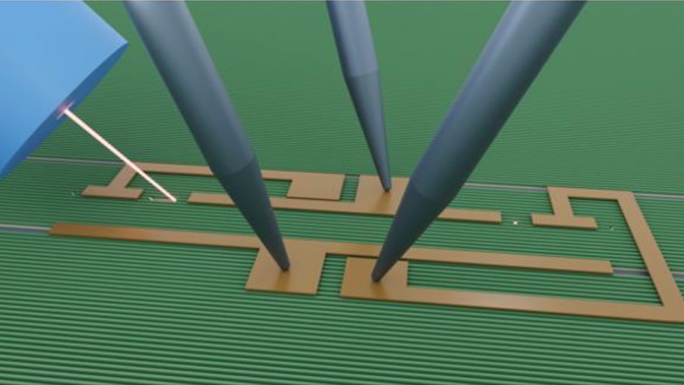
About Miniature Laser Grown on Silicon Chip
- This is a major advancement in the field of silicon photonics, as integrating a light source (laser) directly on the chip has long been a technological challenge.
- Traditionally, lasers are manufactured separately and then attached to chips, which results in slower operation, higher costs, and manufacturing mismatches.
- The new research resolves this issue by growing the laser directly on a silicon chip using a scalable process and compatible with standard CMOS (Complementary Metal-Oxide-Semiconductor) technology, which is the backbone of current semiconductor manufacturing.
- Initially, electrons carried data within silicon chips. However, modern advancements are replacing electrons with photons, leading to the rise of silicon photonics.
- Photons carry information faster, with higher bandwidth and lower energy loss than electrons, making them ideal for next-generation computing, especially in data centres, sensors, and quantum computing.
Photonic Chip Components and Laser Physics
- A photonic silicon chip consists of four key parts:
- A light source (laser),
- Waveguides to channel the photons,
- Modulators to encode or decode data onto light signals, and
- Photodetectors convert light into electrical signals
- The laser functions on the principle of stimulated emission, where electrons drop to a lower energy level, releasing coherent photons to form a laser beam.
However, silicon has an indirect bandgap, making it inefficient at light emission. Therefore, materials like gallium arsenide (GaAs) with a direct bandgap are preferred for laser construction.
- The setup was completed with a protective layer of indium gallium phosphide and electrical contacts to power the laser.
Source: The Hindu
Scientists recently fabricated miniature lasers directly on which of the following material?
A.Graphene
B.Silicon wafers
C.Gallium nitride
D.Quartz
Answer B